Friday, June 19, 2015

What is Thermal Noise?

Thermal Noise is the random fluctuation in voltage caused by the random movement of charge carriers above absolute zero (273K).

 Thermal Noise cannot exist at 273K because charge particles cannot move at absolute zero.

 If the resistor is kept at a temperature above 273 kelvin, thermal noise will be present. Just as a simple experiment, measure the voltage across resistor with the help of CRO. We can see a fluctuating signal above and below the 0V line, This is thermal noise.

The formula to calculate thermal noise of  a resistor is calculated using the below formula

V= Sqrt(4*KTRB) where

K=Boltzman constant
T= Temperature in kelvin
R= Resistance in ohms
B=Bandwidth in Hz where noise is present

Thursday, March 12, 2015

Google App engine | Unsupported major.minor version 52.0

This error will occur when one compiles the Java program using JDK 1.8 and deploys to app engine. The project works fine in the local server, but we get this error while deploying.


Quick Solution:

If you have Java 1.8. Let it be, but also install Java 1.7 and make the changes in the Eclipse as shown below. Also if you are using JSP pages in your project, make sure to check JDK instead of JRE in "Installed JRE's"


I have uploaded the project to app engine without any errors and it works. You can check that here
http://acquitworld.appspot.com/ . I have worked a lot on App engine in the past week so I got to know lot of work around for many errors which will come in the way. So, feel free to ask me. I will be able to help you.


Saturday, January 10, 2015

Analog Electronics (BJT) GATE Previous questions and solutions.

Here are some of Analog Electronics (BJT) GATE Previous questions. The answers can be found in the link at the end of the page.

1)  A Cascade Amplifier Stage is equivalent to
a) A common emitter stage followed by a common base stage
b) A common base stage followed by an Emitter follower
c) An Emitter follower stage followed by a common base stage
d) A common base stage followed by a common emitter stage

2) The cascode amplifier is a configuration of
a) CC-CB b) CE-CB c) CB-CC d) CE-CC

3)  If C3 capacitor is removed from the following circuit. Which of the following statements is true

a) The input resistance Ri increases and the magnitude of voltage gain Av decreases
b) The input resistance Ri decreases and the magnitude of voltage gain Av increases.
c) Both the input resistance Ri and the magnitude of voltage gain Av decreases.
d) Both input resistance Ri and the magnitude of voltage gain Av increase.

4) Identify the type of feedback topology used in the following circuit

a) Voltage-Series
b)Voltage-Shunt
c) Current-Series
d) Current-Shunt

5) If the quiescent collector current Ic, of a transistor increases, then which of the following is true
a) gm will not be affected
b) gm will decrease
c)gm will increase
d) gm will increase or decrease depending upon bias stability.


Solutions :--> Key Answers

Identify the feedback topology of Amplifiers.

 There are four basic feedback topologies. They are
1) Voltage-Series
2) Voltage -Shunt
3) Current- Series
4) Current-Shunt.

But wait, it doesn't stop there. Many textbooks use different nomenclature. So let's see how to get the respective synonyms for the above topologies.
The feedback topologies are also called by the following names.

1) Voltage-Series(Series-Shunt)
2) Voltage -Shunt(Shunt-Shunt)
3) Current- Series(Series-Series)
4) Current-Shunt. (Shunt-Series).


Identify the feedback of Amplifiers.

1) Feedback topology of Non Inverting Amplifer.

Here the feedback signal is derived from Voltage(Voltage driven). The feedback signal is applied as voltage(Series) at the input Hence the feedback topology is Voltage -Series or Series-Shunt.

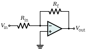
2) Feedback topology of Inverting Amplifier


Here the feedback signal is derived from Voltage(Voltage driven). The feedback signal is applied as 
Current(Shunt). Hence the feedback topology is  Voltage -Shunt or Shunt -Shunt.

Note :

Non-inverting Amplifier uses Voltage Series topology

Inverting Amplifier uses Voltage Shunt topology

Thursday, December 25, 2014

2.5V to 10V Boost Converter simulation

Calculation

Vo=10V
Vi=2.5V

For Boost Converter, the duty cycle of the pulse required is D=1-(Vi/Vo)=0.75

It is normal to operate coils at a frequency which is not perceived by the human ears. so let's keep the frequency at 20kHz . i.e the switch is operated at this frequency.

The above equation of duty cycle is valid only if the boost converter is operated in continuous mode. i.e Inductor current never falls to zero.

To make sure of that, the inductance of inductor should be greater than the inductance L

L=D*(1-D)*(1-D)*R/(2*f)
=0.75*0.25*0.25*100/(2*20000)

L=117uH. We have chosen a value of 200uH to make sure the below converter operates in continuous mode. 


The output capacitor C required to limit the output ripple voltage to 1 percent is determined

C>=D/(R*0.01*f)=37.5uf. I have chosen a standard 47uf.

Note: The Duty cycle has been calculated assuming that voltage drop across the diode is 0V. But the diode used in the above circuit has practical voltage across it. So we have made duty cycle as 77 here to get the required output voltage.

The Simulation can be found out here -->http://tinyurl.com/qgao6jy

Sunday, December 14, 2014

Difference between diffusion capacitance and depletion/transition capacitance

The reactance of a capacitor is given by Xc=1/2*pi*f*C. At lower frequency, Xc is very very large and we can treat it as open circuit. However, at high frequencies, the Xc value becomes smaller and significant and we will not be in the position to ignore. While dealing with the electronic devices at higher frequencies, two capacitance come into picture. They are

1) Diffusion Capacitance
2) Depletion Capacitance, also called as transition capacitance.

Difference between diffusion capacitance and depletion/transition capacitance

  1. Depletion Capacitance


Depletion capacitance will be dominant  in reverse bias region.

The capacitance of a parallel plate capacitor is given by C =εA/d.

Under reverse bias condition, the depletion region acts as  a parallel plate capacitor with the depletion region width as d, and it's effective area as A in the above equation.

Depletion width(d) increases when the reverse bias voltage increases, so the depletion capacitance  decreases with increase in reverse bias voltage.

2. Diffusion Capacitance

Diffusion Capacitance will be dominant in forward bias condition.

CD = τID / ηVT where VT=KT/q

The diffusion capacitance decreases with decreasing current and increasing temperature.


Note: Both this capacitance will come into picture at higher frequencies and one can ignore them at lower frequencies.


Semiconductor theory | Reverse saturation current and forward bias voltage

The behavior of PN junction is different for reverse saturation current and forward bias voltage when the temperature is increased. Let's study the behavior of PN junction with examples.


Q) A Silicon PN junction at a temperature of 20 degree celsius has a reverse saturation current of 10pA. The reverse saturation current at 40 degree celsius for the same bias is approximately

Ans : 40 pA. Reverse saturation current doubles for every 10 degree rise in temperature

At 20 degree celsius-->10pA
At 30 degree celsius  --->20pA
At 40 degree celsius --->40 pA.


Q) A Silicon PN junction biased with a constant at room temperature. When the temperature is increased by 10 degree celsius, the forward bias voltage across the junction decreases by?
Ans : Decreases by 25mV


For every degree rise in temperature, the voltage decreases by 2.5mV.

For 10 degree rise in temperature ---> 2.5mV*10=> Voltage decrease by 25mV