Saturday, July 19, 2014

Create a frequency using 8051 Microcontroller. Timer 0 Mode 1. Proteus simulation

8051 has two timers. Timers can be used to generate delay. So, we can create pulse of various frequencies using 8051. Let's see as how to create a frequency on particular pin of microcontroller, 8051. We will use proteus simulation to demonstrate the same.

                                                         Circuit diagram


Here is the code, which generates a frequency of 10Hz on pin  P2.7.

Code :
#include "reg52.h"
#define Baud_rate 0xFD  // BAUD RATE 9600                     
void delay(void);
sbit App = P2^7;


void main()
{ 
while(1)
 {
 App=~App; //To generate a pulse(ON/OFF)
 delay();
 }
}

void delay(void)
{
  TMOD=0x01;      //Timer 0 mode 1
  TL0=0xFD; 
  TR0=0x4B;
  TR1=1;         //start timer
  while(TF1==0); //Timer flag
  TR1=0;         //reset timer
  TF1=0;
}


The Microcontroller used here has a crystal frequency of 11.0592MHz. 
In order to generate a Frequency of  10Hz, we need to use timer registers.
The steps to load values into TH and TL registers which generate delay are as follows
1) Divide the desired time delay by 1.085us. Here delay is 1/10=100ms. So, 100ms/2=50ms/1.085us=46083
2) Perform 65536-delay=65536-46083=19453
3)Convert the value obtained in the above step to Hex.  19453 is in decimal, in Hex, the value is 4BFD.
4)Load TH=4B
5)Load TL=FD
when you start the timer, the timer registers will count till FFFF generating the desired delay. Thus generating a pulse of required frequency/delay.

Friday, July 18, 2014

Send data from 8051 to Hyperterminal (PC/Computer)

My first post here was http://www.hobbyprojects.in/2013/03/serial-communication-between-pc-and-8051.html which went  viral. I had also made a video on sending data from 8051 to Hyperterminal(which will be present in PC). The video  was missing in the website. We will see in detail , the serial communication between Microcontroller and Hyperterminal.

How to send data from Microcontroler to Hyperterminal ?

Detailed Circuit diagram
The circuit consists of Microcontroller, Max232, COMPIM, inverters and virtual terminal as shown in the figure. We have used Free virtual serial ports emulator so that we can connect two or three communication ports together.

 Make the port of COMPIM as COM4. The data sent from Microcontroller will flow via COM4.

 Since, the Hyperterminal doesn't have many ports inbuilt, we will use virtual ports emulator to get the ports. Here we have connected COM2 and COM4 in pair. The data sent from COM4 will also flow through COM2 as they are connected.
 

Hyperterminal will be in the following in the computer. Start->All programs--> Accessories-->Communications-->Hyperterminal
 Here the port via which the hyperterminal makes communication with microcontroller is COM2.
Set the properties. Baud Rate should be as defined in 8051

Click on Echo typed characters locally
The data sent from Microcontroller will be displayed on Hyperterminal. Start the simulation, you can see the output in virtual terminal as shown below.


 The actual data, "Hello" which is transferred from Microcontroller (8051) to PC/Computer will be displayed in the hyperterminal. Thus, the data is successfully transmitted from 8051 to Hyperterminal.


 I have made a video too. Please watch here. The code is simple, if anyone needs the code. Please use the comment box. Thanks.


Saturday, June 14, 2014

Current Mirror with Emitter degeneration resistors

No circuit element has contributed to the " STABILITY of ANALOG CIRCUIT" as much as Emitter degeneration resistors. Especially when you are dealing with BJT, a lot of factors decide the working of the circuit such as Beta value of transistor, temperature etc. If circuit characteristics change w.r.t any of the temperature, beta etc cannot be considered as a stable circuit.

   Then what has to be done to make circuit independent of all those external factors?
Soln: Most of the time, Emitter degeneration resistor acts as a savior. In this post, we will see how emitter degeneration resistor(s) decide the overall working pattern of a current mirror.

 Here is a sample circuit

This is the popular current mirror circuit with 2 EMITTER DEGENERATION RESISTORS R1 and R2.

As you can see. VB1=VB2( The base of two BJT's are connected to each other).
The Red Probe will show the current of Q1 transistor in simulation. Let's call the collector current of Q1 as I1
The Green Probe will show the current of Q2 transistor in simulation . Let's call the collector current of Q2 as I2.
*Neglecting base current*
By using Simple KVL,
VB1=VB2
VBE1+I1*R1=VBE2+I2*R2

Assuming both BJT's are fabricated at a same time under same conditions(Which isn't the case practically, so there will be a slight error in calculation). Let's assume VBE1=VBE2

In that case, I1*R1=I2*R2

I1/I2=R2/R1.       

 I2= I1*(R1/R2). 

Since we are dealing with BJT's calculating current is little tedious, so lets concentrate on ratios of two currents I1 and I2 as shown by Red and green probe respectively.

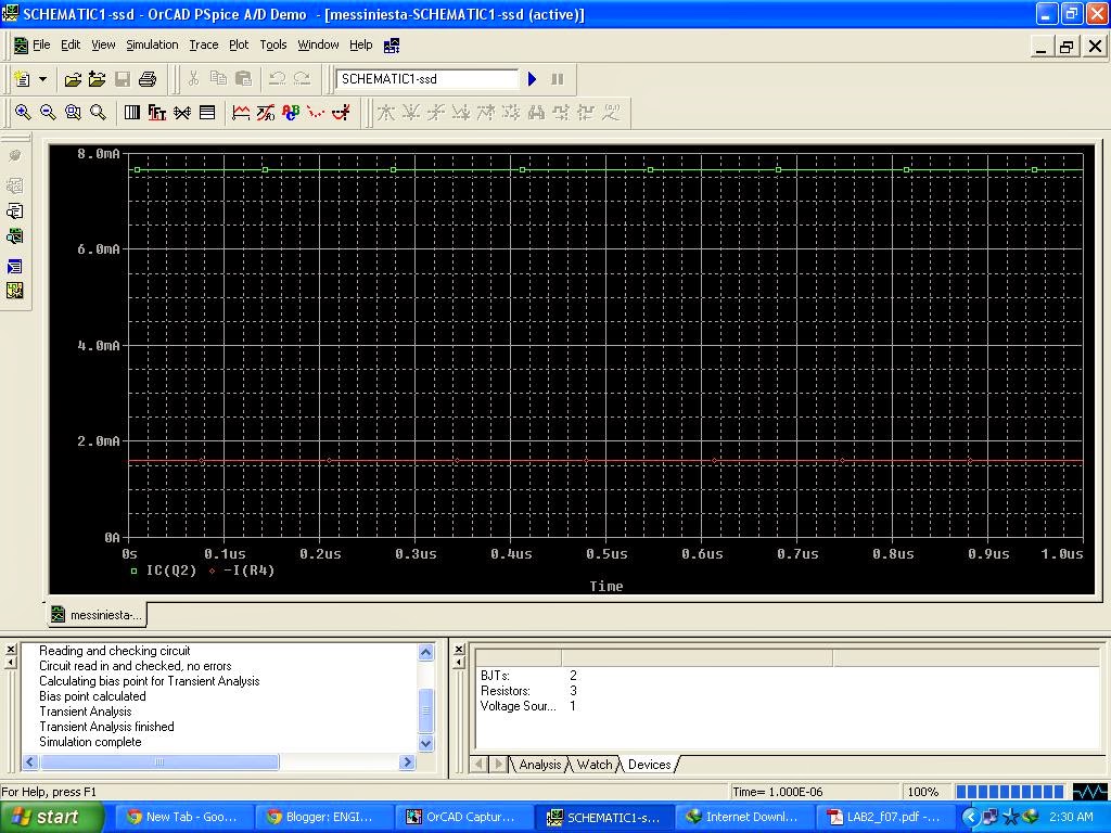
In the above circuit, R1=5k and R2=1k. So , I2=5*I1. which you can see below. The mirrored current totally depends on emitter degeneration resistor and doesn't change with the Beta value of BJT or the temperature.


I2=7.6mA and I1=1.6mA. I2 is 5 times(Almost)


In the below circuit. R1=8k and R2=1k, So I2 should be 8 times I1 and you can see that I2 is 8 times I1.


In this post, we demonstrated the simple effect of emitter degeneration resistor. For any doubts, contact us via comment box or the email id. 

Sunday, June 1, 2014

BICMOS NOR GATE


This is the schematic of BICMOS NOR Gate. I have explained in detail, the working of  BICMOS NAND GATE .This post will make the concept clear and also you have the schematic of BICMOS NOR GATE.

Logic

A B Y

0 0 1
0 1 0
1 0 0
1 1 0

1) When both A and B are 0. Both the PMOS will be ON. The base of Q1 will be VDD , say 5v. The base of Q1 is also connected to the GATE of bottom NMOS.  So, bottom NMOS is ON and it removes the base charge of Q2, if any and makes sure that Q2 is OFF. when A=0, B=0, Q1 is ON and Q2 is OFF.

BICMOS NOR GATE  has characteristics of both CMOS and BJT's . CMOS have ZERO STATIC POWER DISSIPATION and BJT's have HIGH TRANSCONDUCTANCE(High speed logic families). Also, BJT's have large current driving capability.

2) For other permutations of input.

For other inputs, the BASE charge of Q1 is removed by the 2  NMOS. The bottom NMOS is off and the output is pulled to Zero.


Note:  CMOS is by far, the best logic family. CMOS have zero static power dissipation, but BJT's are still imperious in terms of Speed.( ECL , still stands top as the high speed logic family). BJT's also have a large current driving capability, which MOSFET doesn't have. In order to have same current driving capability of that of BJT's , MOSFET SIZE needs to be significantly increased.

In order to incorporate both the advantages of CMOS and BJTs, BICMOS has been invented(Discovered, more aptly).  Still, it involves lot of mess to fabricate BICMOS. Nevertheless, BICMOS is one of the important logic family.


 For any doubts on BICMOS LOGIC Family, please contact us or use the comment box.


Saturday, May 10, 2014

Working of BICMOS NAND GATE

There are many logical families such as RTL, DTL, ECL, CMOS etc.
All have their advantages and disadvantages. However, in the past decade, CMOS is ruling the electronics field because of its SIZE and POWER.

Did you know that ?

CMOS(Complementary metal oxide semiconductor) has ZERO static power dissipation. However, The switching speed of CMOS is very low compared to BJT, and also CMOS cannot drive large current to the load. In order to drive large current to the load, the size of MOS needs to be significantly increased.

Is there a logical family which incorporates the advantages of both CMOS and BJT?

Ans : Yes, and that logical family is called BICMOS.

        How to draw BICMOS ? How different it is from normal CMOS gates?

 We shall see BICMOS NAND GATE.
This is the two input BICMOS NAND gate.

It consists of
1) 2 PMOS PA and PB
2) 4 NMOS, NA1, NB1, NA3, NB3
3) Two BJT's QP and Q0


NAND GATE

A    B     Y
0    0      1
0    1      1
1    0      1
1    1      0


Case 1 : Both A and B are low.

If both the inputs VA and VB(Refer the circuit) are low(0). PA and PB will be ON and the base of QA will be high. THus the top BJT(QA) will be ON which pulls the output UP . If there is a capacitive load. The output current will be almost 101 times the base current i.e it will be 101IB(Assuming beta of transistor is 100). (if there was no BJT, the output current would be just IB).

Note: PA, PB, NA1 and NB1 are used for logical purposes(Just like in CMOS)

What is the purpose of N2, NB3 and NA3?

For high switching speeds of the BJT's, we need to remove the base charge from the transistor. In order to remove the charge from the base of the transistor we need a mechanism, that can be achieved by using these 3 NMOS. 

Why to remove the Base charge anyway?

If we do not remove the base charge, the transistor will be in ON state and takes a lot of time to go to the OFF state. If we do not remove the base charge, the whole purpose of BICMOS is lost.

 N2 MOS is getting input from the base of QA transistor. Since the base of QA is HIGH(say 5v), it will on N2 MOS. Since N2 is ON, it will PULL THE BASE CHARGE OUT OF Q0 transistor. So, if both the inputs are low, QA is ON and Q0 is OFF. OUTPUT IS HIGH and OUTPUT CURRENT IS LARGE. HIGH SWITCHING SPEED.


Case 2 : A and B are high

NB3 and NA3 NMOS make sure that QA is in OFF state. PA and PB are OFF. NB1, NA1 will be ON. The output is discharged via NB1, NA1 and Q0.(High Speed). N2 will be effectively out of circuit in this case. So, Q0 is ON and QP is OFF.

I have discussed 2 cases. You can correlate with the other 2 inputs.

Disadvantages of BICMOS
1) Fabrication cost is high
2) Due to VBE(Base to emitter voltage, 0.7v approximately) of BJT's , desirable performance is not obtained when the BICMOS gates are operated at lesser voltages (3V, 2.4V) etc.

For any Queries, please use the comment box. ADIOS!

Friday, March 7, 2014

How to draw BODE PLOT In MATLAB!

Suppose take a transfer function

G(S) H(S)= 10/(S+1)

To plot a Bode Plot for this Transfer function. 

Open Matlab .
In the command window, write the co-efficients of S^2  and S as well as constant.

Following this rule, we shall write the numerator of G(S) H(S) as num=[0 0 10] , which means numerator only contains a constant i.e 10 .S^2 and S are absent

Coming to the denominator of G(S) H(S)=[0 1 1], which means denominator doesn't contains S^2, and co-efficient of S is 1 and the constant is 1.  


Figure 1


Bode plot of above TF can be drawn in Matlab using matlab command Bode(num,den) as shown above.

Bode Plot :
Figure 2


The transfer function G(S) H(S)=10/S+1 is a Single Pole transfer function.

Here  cutoff Frequency wc=1/(coefficient of S) is 1 rad/sec.

As you all know actual bode plot differs from the approximation bode plot by -3dB as shown below
Figure 3

REFER TO FIGURE 2
 We can see  that, at the cut-off frequency or  at the POLE, the Magnitude plot at the pole location varies by -3dB  i.e (20dB-3dB=17 dB. Hence We can conclude that Matlab gives actual Bode plot.
Feel free to ask any questions. We shall see few more Transfer functions in the next post.