Friday, June 19, 2015

What is Thermal Noise?

Thermal Noise is the random fluctuation in voltage caused by the random movement of charge carriers above absolute zero (273K).

 Thermal Noise cannot exist at 273K because charge particles cannot move at absolute zero.

 If the resistor is kept at a temperature above 273 kelvin, thermal noise will be present. Just as a simple experiment, measure the voltage across resistor with the help of CRO. We can see a fluctuating signal above and below the 0V line, This is thermal noise.

The formula to calculate thermal noise of  a resistor is calculated using the below formula

V= Sqrt(4*KTRB) where

K=Boltzman constant
T= Temperature in kelvin
R= Resistance in ohms
B=Bandwidth in Hz where noise is present

Thursday, March 12, 2015

Google App engine | Unsupported major.minor version 52.0

This error will occur when one compiles the Java program using JDK 1.8 and deploys to app engine. The project works fine in the local server, but we get this error while deploying.


Quick Solution:

If you have Java 1.8. Let it be, but also install Java 1.7 and make the changes in the Eclipse as shown below. Also if you are using JSP pages in your project, make sure to check JDK instead of JRE in "Installed JRE's"


I have uploaded the project to app engine without any errors and it works. You can check that here
http://acquitworld.appspot.com/ . I have worked a lot on App engine in the past week so I got to know lot of work around for many errors which will come in the way. So, feel free to ask me. I will be able to help you.


Saturday, January 10, 2015

Analog Electronics (BJT) GATE Previous questions and solutions.

Here are some of Analog Electronics (BJT) GATE Previous questions. The answers can be found in the link at the end of the page.

1)  A Cascade Amplifier Stage is equivalent to
a) A common emitter stage followed by a common base stage
b) A common base stage followed by an Emitter follower
c) An Emitter follower stage followed by a common base stage
d) A common base stage followed by a common emitter stage

2) The cascode amplifier is a configuration of
a) CC-CB b) CE-CB c) CB-CC d) CE-CC

3)  If C3 capacitor is removed from the following circuit. Which of the following statements is true

a) The input resistance Ri increases and the magnitude of voltage gain Av decreases
b) The input resistance Ri decreases and the magnitude of voltage gain Av increases.
c) Both the input resistance Ri and the magnitude of voltage gain Av decreases.
d) Both input resistance Ri and the magnitude of voltage gain Av increase.

4) Identify the type of feedback topology used in the following circuit

a) Voltage-Series
b)Voltage-Shunt
c) Current-Series
d) Current-Shunt

5) If the quiescent collector current Ic, of a transistor increases, then which of the following is true
a) gm will not be affected
b) gm will decrease
c)gm will increase
d) gm will increase or decrease depending upon bias stability.


Solutions :--> Key Answers

Identify the feedback topology of Amplifiers.

 There are four basic feedback topologies. They are
1) Voltage-Series
2) Voltage -Shunt
3) Current- Series
4) Current-Shunt.

But wait, it doesn't stop there. Many textbooks use different nomenclature. So let's see how to get the respective synonyms for the above topologies.
The feedback topologies are also called by the following names.

1) Voltage-Series(Series-Shunt)
2) Voltage -Shunt(Shunt-Shunt)
3) Current- Series(Series-Series)
4) Current-Shunt. (Shunt-Series).


Identify the feedback of Amplifiers.

1) Feedback topology of Non Inverting Amplifer.

Here the feedback signal is derived from Voltage(Voltage driven). The feedback signal is applied as voltage(Series) at the input Hence the feedback topology is Voltage -Series or Series-Shunt.

2) Feedback topology of Inverting Amplifier


Here the feedback signal is derived from Voltage(Voltage driven). The feedback signal is applied as 
Current(Shunt). Hence the feedback topology is  Voltage -Shunt or Shunt -Shunt.

Note :

Non-inverting Amplifier uses Voltage Series topology

Inverting Amplifier uses Voltage Shunt topology

Thursday, December 25, 2014

2.5V to 10V Boost Converter simulation

Calculation

Vo=10V
Vi=2.5V

For Boost Converter, the duty cycle of the pulse required is D=1-(Vi/Vo)=0.75

It is normal to operate coils at a frequency which is not perceived by the human ears. so let's keep the frequency at 20kHz . i.e the switch is operated at this frequency.

The above equation of duty cycle is valid only if the boost converter is operated in continuous mode. i.e Inductor current never falls to zero.

To make sure of that, the inductance of inductor should be greater than the inductance L

L=D*(1-D)*(1-D)*R/(2*f)
=0.75*0.25*0.25*100/(2*20000)

L=117uH. We have chosen a value of 200uH to make sure the below converter operates in continuous mode. 


The output capacitor C required to limit the output ripple voltage to 1 percent is determined

C>=D/(R*0.01*f)=37.5uf. I have chosen a standard 47uf.

Note: The Duty cycle has been calculated assuming that voltage drop across the diode is 0V. But the diode used in the above circuit has practical voltage across it. So we have made duty cycle as 77 here to get the required output voltage.

The Simulation can be found out here -->http://tinyurl.com/qgao6jy

Sunday, December 14, 2014

Difference between diffusion capacitance and depletion/transition capacitance

The reactance of a capacitor is given by Xc=1/2*pi*f*C. At lower frequency, Xc is very very large and we can treat it as open circuit. However, at high frequencies, the Xc value becomes smaller and significant and we will not be in the position to ignore. While dealing with the electronic devices at higher frequencies, two capacitance come into picture. They are

1) Diffusion Capacitance
2) Depletion Capacitance, also called as transition capacitance.

Difference between diffusion capacitance and depletion/transition capacitance

  1. Depletion Capacitance


Depletion capacitance will be dominant  in reverse bias region.

The capacitance of a parallel plate capacitor is given by C =εA/d.

Under reverse bias condition, the depletion region acts as  a parallel plate capacitor with the depletion region width as d, and it's effective area as A in the above equation.

Depletion width(d) increases when the reverse bias voltage increases, so the depletion capacitance  decreases with increase in reverse bias voltage.

2. Diffusion Capacitance

Diffusion Capacitance will be dominant in forward bias condition.

CD = τID / ηVT where VT=KT/q

The diffusion capacitance decreases with decreasing current and increasing temperature.


Note: Both this capacitance will come into picture at higher frequencies and one can ignore them at lower frequencies.


Semiconductor theory | Reverse saturation current and forward bias voltage

The behavior of PN junction is different for reverse saturation current and forward bias voltage when the temperature is increased. Let's study the behavior of PN junction with examples.


Q) A Silicon PN junction at a temperature of 20 degree celsius has a reverse saturation current of 10pA. The reverse saturation current at 40 degree celsius for the same bias is approximately

Ans : 40 pA. Reverse saturation current doubles for every 10 degree rise in temperature

At 20 degree celsius-->10pA
At 30 degree celsius  --->20pA
At 40 degree celsius --->40 pA.


Q) A Silicon PN junction biased with a constant at room temperature. When the temperature is increased by 10 degree celsius, the forward bias voltage across the junction decreases by?
Ans : Decreases by 25mV


For every degree rise in temperature, the voltage decreases by 2.5mV.

For 10 degree rise in temperature ---> 2.5mV*10=> Voltage decrease by 25mV 

Friday, November 28, 2014

Maxwell Equations and Light

 And Maxwell said


and there was Light.


Sunday, November 16, 2014

How to draw Root Locus diagram?


1) There are 4 poles and no zeros. P=4 and Z=0. N=4. There will be 4 branches in root locus

2) All 4 branches will start from open loop poles and terminate at infinity.

3) The branches will terminate at infinity along straight line asymptotes whose angles are determined by

where q=0..N-1

Angle of asymptotes =45, 135,225,315


4) The asymptotes meet the real axis at Centroid

Centroid= Sum of real parts of poles-sum of real parts of Zeros/(P-Z)=0-1-2-3/4=-1.5

5) Breakaway point and Break in  point  is calculated by solving dk/ds=0


Solving this gives s=-1.5, -0.381, -2.619. (Note : -1.5 is not valid breakaway point point because it doesnt lies on root locus)

6) The value of k and the point at which the root locus branch crosses the imaginary axis is determined by applying Routh Criterion to the characteristic equation. The roots at the intersection point are imaginary.


 s^4 | 1     11          k

 s^3 | 6       6            0

 s^2 | 10         k          0   

 s^1 | (60-6k)/10   0       

 s^0 |   k                        

60-6k=0 --> kmax=10

Auxiliary  equation : 10s^2+k=0

At k=10, s=+j and s=-j                  


7) Root Locus 
  
Root Locus plot

This is the root locus diagram for the given transfer function

Summary

The system is absolutely stable for 0<k<10 and at k=10, the system is marginally stable and for k>10, system is unstable.

Sunday, November 9, 2014

Different types of Controllers in Control System

1) Proportional Controller : Transfer Function of proportional controller is G(s)=Kp. Mainly used to vary transient response of a system

2) Integral Controller : Transfer function of Integral controller is Gc(s)=KI/S. It is used to decrease steady state error of a system. But in doing so, the stability of a system decreases

3) Derivative Controller : G(s)=KD*S. It is opposite of Integral controller. It is used to increase the stability of a system. The stability of a control system can be enhanced by adding ZEROS. And since the type of a system decreases, the steady state error increases.

4) PI Controller : G(s)=Kp+ KI/S= (SKp+KI)/S. This controller will reduce the steady state error without effecting stability.

5) PD Controller : G(S)= KD.S+Kp. This controller is used to increase the stability without effecting steady state error. Since type is not changed and a zero is added.

6) PID controller = Kp+ KD.S+ KI/S

 It is used to increase the stability and decrease the steady state error of the control system.

Thursday, November 6, 2014

How Edwin Armstrong became the most influential person in radio history


The Germans were using certain high frequency signals to communicate with each other during world war 1. 

During that time, if the other countries wanted to know, well in advance as ' what the Germans are planning', they had to receive the signal and amplify it accordingly. The plan would be to design a tuned filter. Back in the days, it was easy to build a receiver circuit to track the signal, but there wasn't a proper Amplifer. 

Why Amplifier?
  Amplifier is a device which increases the voltage, current or power of the signal. In common terms, to increase the volume of the signal(Voice supposedly).

   When United States entered world war 1, Armstrong joined Army signal corps and was sent to Paris, and was placed in charge of Research section. While travelling to France, Armstrong met captain H.J Round, an engineer with British Marconi Company. Armstrong learned that the British were ahead of Americans in development of Vaccum tables capable of handling frequency signals ranging from 500KHz to 3.5MHz, a frequency range that it was suspected, the Germans were using for communication. In that way, the British had kept track of many Germany ships and also had broken their codes and nearly read all the messages.

 Germans continued to communicate with each other from different ships planning the destruction of allied countries.  Americans tried to read those messages, but ultimately fell short to build a proper receiving circuit/Amplifier stage and were like
Can't hear anything. Increase the volume


They appointed Armstrong and assigned him to detect short wave enemy communication.


Armstrong realized that if radio direction-finding (RDF) receivers could be operated at a higher frequency, this would allow better detection of enemy shipping. However, at that time, no practical "short wave" (defined then as any frequency above 500 kHz) amplifier existed, due to the limitations of existing triodes.


It had been noticed some time before that if a regenerative receiver was allowed to go into oscillation, other receivers nearby would suddenly start picking up stations on frequencies different from those that the stations were actually transmitted on. Armstrong (and others) eventually deduced that this was caused by a "supersonic heterodyne" between the station's carrier frequency and the oscillator frequency. Thus if a station was transmitting on 300 kHz and the oscillating receiver was set to 400 kHz, the station would be heard not only at the original 300 kHz, but also at 100 kHz and 700 kHz.
Armstrong realized that this was a potential solution to the "short wave" amplification problem, since the beat frequency still retained its original modulation, but on a lower carrier frequency. To monitor a frequency of 1500 kHz for example, he could set up an oscillator at, for example, 1560 kHz, which would produce a heterodyne difference frequency of 60 kHz, a frequency that could then be more conveniently amplified by the triodes of the day. He termed this the "Intermediate Frequency" often abbreviated to "IF".
The signal with intermediate frequency had retained its original modulation(It means, "The secret message" was still encrypted in the carrier signal, albeit on a lower frequency). 

But there was an advantage this time, the united states Army had proper equipment(Amplifier) to amplify the signals in the IF frequency range which was not the case in the short wave range.

The Military of US adopted the methodology and were able to increase the volume of signal(Amplify) and were able to hear 'what the Germans were planning'?.


If you are wondering how superheterodyne receiver looks like. Here you go.


One of the important advantages of Superheterodyne receiver is  : Irrespective of the frequency transmitted by any station, the IF(Intermediate frequency) remains same, so the amplifier design remains robust and doesn't depend on the frequency of the station.

Almost all modern radio receivers employ this method and even today, Edwin Armstrong is regarded as one of the greats in Radio history.


Wednesday, November 5, 2014

Frequency Modulation examples/problems

1) A music signal with frequency components from 50 Hz to 21000 Hz is Frequency modulated.  If the maximum allowed frequency deviation is 50 kHz. (i)       What is the modulation index?
ii)What is the signal bandwidth using Carson’s rule?

Solution: i) Modulation index = frequency deviation/modulating frequency = 50 kHz/21 kHz = 2.38
               
(ii) Bandwidth is 2 (modulating frequency + frequency deviation) = 2 (21 kHz + 50 kHz) = 142 kHz

2)A 200 MHz carrier is frequency modulated by a 10 V peak-to-peak signal of 10 kHz. The instantaneous carrier frequency varies between 199.90 and 200.10 MHz.
 Calculate (i) The modulator sensitivity.
                        (ii) The modulation index.
                        (iii) The signal bandwidth using Carson’s rule.

(i)

2 * Frequency deviation = 200.10 – 199.9 MHz = 200 kHz.
Frequency deviation = 100kHz
This is caused by a 10 V signal.
Therefore sensitivity is 100/10 kHz/V = 10 kHz/V

(ii)

The modulation index is 200 kHz / 10 kHz = 20.

(iii)
BW      =          2 (frequency of modulating signal + frequency deviation)                
            =          2 ( fm + k * fd)                                                                                     
            =          2 ( 1 + b ) * fm                                                                                     

Using any of the above

            BW = 420kHz


  3) A speech signal with frequency components from 300 Hz to 4 kHz is Frequency modulated.  If the maximum allowed frequency deviation is 30 kHz
(i)                 What is the modulation index?
(ii)               What is the signal bandwidth using Carson’s rule?
(i)
Modulation index = frequency deviation/modulating frequency = 30 kHz/4 kHz = 7.5

(ii)
Bandwidth is 2 (modulating frequency + frequency deviation) = 2 (30 kHz + 4 kHz) = 68 kHz

Friday, October 24, 2014

Need for Modulation


1) To reduce Antenna height

The antenna height required to transmit a signal is proportional to operating wavelength. For efficient transmission, the minimum antenna height required should be lambda/4. So if we want to transmit a low frequency signal(f), we have v=f*lambda. lambda is inversely proportional to frequency, so low frequency means large wavelength(lambda)--> Antenna required will be very high. Modulation converts the given signal to high frequency signal.

2) To reduce noise

The effect of noise will be more at some frequencies and the effect will be less at some other frequencies. Modulation shifts the spectrum to other band of frequencies where noise effect will be less.

3) Conversion of bandlimited signal to narrowband signal

 Modulation converts a bandlimited signal to a narrowband signal that has ratio between highest frequency to lowest frequency less, so that we can transmit a signal with single antenna which wouldn.'t be possible if the ratio was high.(Which is the case if modulation is not performed on the respective signal)

4) Multiplexing

More than one signal can be transmitted through the same communication channel. By modulation it is possible. We will see about it in detail in the coming posts.
\


Wednesday, October 22, 2014

Transient analysis of RLC/RL/RC circuit- PSPICE Simulation

In this post, we will see the transient analysis of RL circuit with the help of an example. Before solving that we should understand the behaviour of Inductor in the steady state condition. To know in detail. See this video--> Prerequisite

Let's take the following example

 PSPICE simulation of RLC circuit
Main diagram


A) Before t=0-

In the above example, before t=0-, i.e in a steady state condition, inductor will act as a short circuit, so the current through the inductor at t=0- will be 0.75A. i(t), in this case will be 0.

B) At t=0+

After the switch S is closed, the inductor will resist the change, so it will not permit this to happen. Even after the switch is closed at t=0. At t=0+(Just after the switch is closed), inductor will still take 0.75A. So the two resistors which are in parallel divide the remaining 0.75A among themselves. i.e i(t)=0.375A at t=0+.


c) t=0+ to infinity

The inductor is a memory element, so it resists the change in current. It takes certain time to reach a steady state. At steady state(t=infinity), the current through il=0.5A(Since L acts a short circuit, the above circuit will be just  a parallel combination of 3 resistors each of 10 ohm. i(t) |t=infinity=0.5A.

General expression of i(t) can be found using the following equation(Refer main diagram to know which is i(t))

i(t)=Final value+(Initial Value-Final value) exp(-t/tc)  ,where tc=time constant of a circuit.

so, 
i(t)=0.5+(0.375-0.5) exp(-1000t) A.

i(t)=0.5-0.125*exp(-1000t) A.

At t=0, i(t)=0.375A
At t=infinity, i(t)=0.5A


                                              PSPICE SIMULATION


i(t)

iL

Red color=i(t). Green color=iL


Note

Because of the presence of inductor, the current i(t) takes certain time(5 time constant) to reach its final value of 0.5A. The current i(t) value varies from 0.375A to 0.5A .
Inductor resists the change in the current.


Simulation video--> Part 1 and Part 2

Saturday, October 11, 2014

Control System Quiz

1) The transfer system of the system which will have more steady error for unit step input is
a) 80/(s+1)(s+2)(s+3)
b)120/s(s+1)(s+15)
c) 60/(s+0.5) (s+3)(s+5.5)
d)120/(s+1)(s+4)(s+15)
Show/hide solution

2)When the gain 'K' of the system is increased, the steady state error of the system
a)Increases
b) Decreases
c) Remains unchanged
d) May Increase or decrease
Show/hide solution

3)A unity feedback system has forward path transfer function G(s)=K/s(s+2). If the design specification is that the steady state error due to ramp input is 0.05,the value of K allowed is
a)20
b)40
c)10
d)80
Show/hide solution

Friday, August 15, 2014

Mason's gain formula example

Control Systems is a fantastic subject and I wanted to write some topics regarding that. The first thing you notice in control system class is to find the gain of a "PRETTY BIG BLOCK" by using various reductions techniques. The steps involved will be :
1) Multiply the gain(G) of the blocks which are in series and add the gains(G) which are in parallel
2) Switch the take-off point to the right side of the block and blah-blah stuff. 

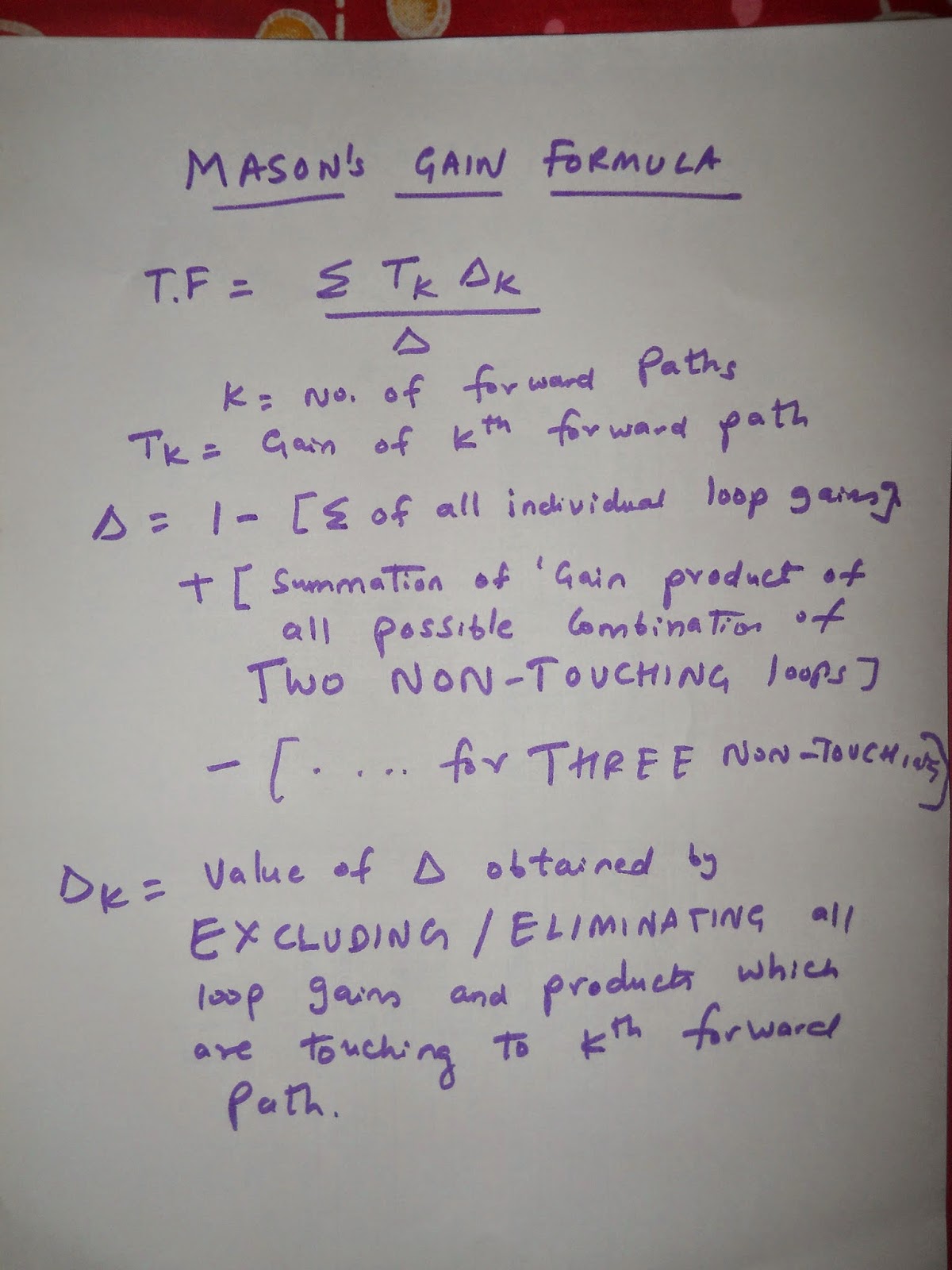
So, in order to avoid all these steps, one brilliant lad, invented a formula, which is named after him(We are accustomed to FORMULA, isn't it? ). That formula makes life easy for us who study control system. That formula is called, MASON'S GAIN FORMULA. Mason's gain formula applies only to LINEAR SYSTEMS.

If you don't know what Linear System is? Google has a quick ans : A general deterministic system can be described by operator, H, that maps an input, x(t), as a function of t to an output, y(t), a type of black box description. Linear systems satisfy the properties of superposition and scaling or homogeneity.


Mason's gain formula Example.

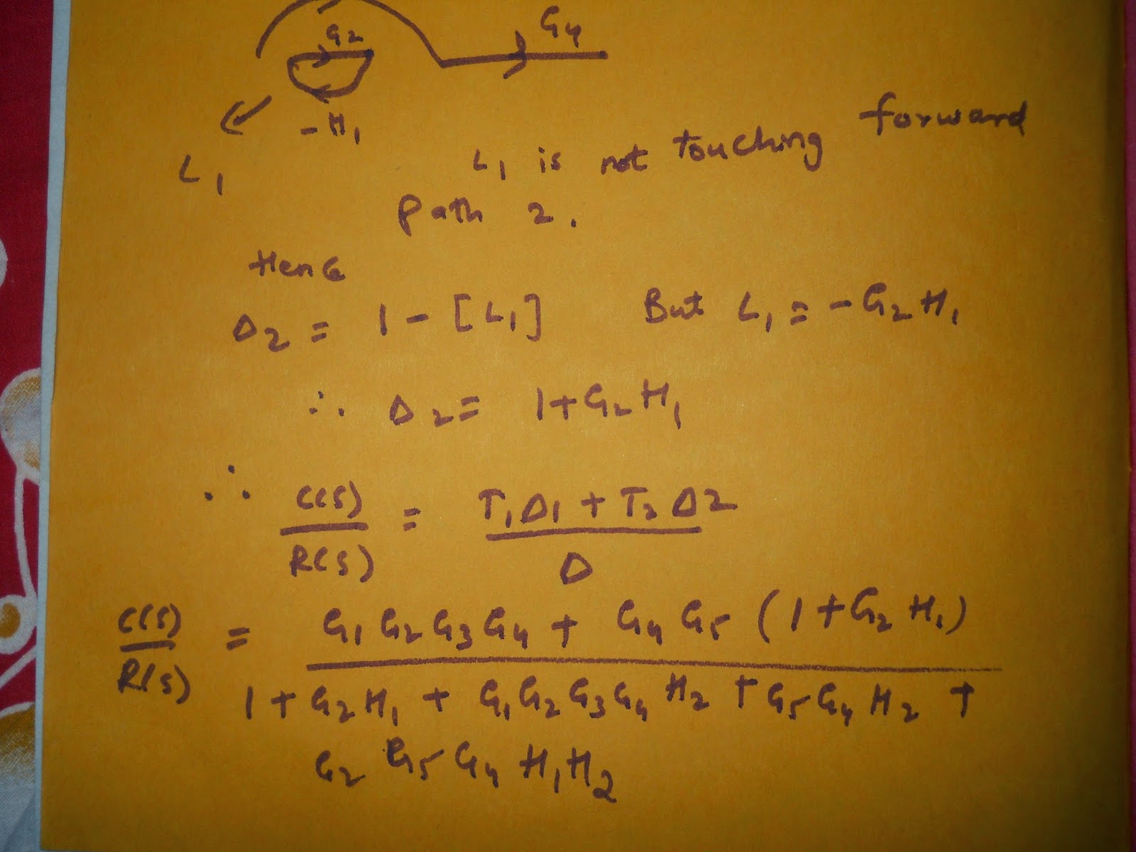
I have solved  a Signal Flow graph using Mason's gain formula. The explanation would be suffice I guess. Kindly go through the snapshots and revert back for any doubts.
Tip:Zoom the pic for better clarity

Mason gain formula example